
Andy Pye takes a futuristic look at some on-going developments in how the electronic and other properties of polymers are being tailored for specific purposes.
A generation ago, polymer design involved a top-down approach – selecting the optimum material from a range of engineering polymer options supplied in bulk by a limited number of suppliers. That approach largely remains true today, but we are now seeing the development of highly tailored polymeric materials whose properties are being designed from scratch to meet the demands of particular applications – a special type of reverse engineering, if you will.
These so-called functional materials have a very specific portfolio of properties and are very specialised; while they are certainly not cheap to produce, in certain circumstances the value they impart to the application easily justifies the development effort and the price to the customer. Here are some examples of bottom-up polymer design in action.
Biodegradable circuit boards for wireless communications
Engineers from a Scottish university are teaming up with an industrial company to develop environmentally-friendly, biodegradable circuit boards for use in wireless communication technologies.
The partnership between the University of Glasgow and Jiva Materials aims to cut down on the electronic waste produced by traditional printed circuit boards (PCBs).
PCBs account for up to 40% of the world’s waste electrical and electronic equipment. Conventional PCBs, which use flame-retardant composites or ceramics, are impossible to recycle and are routinely sent to landfill.
Additionally, more advanced circuits often contain ‘forever chemicals’ like PFAs, which cause harm to the environment, humans and animals when they leach into groundwater.
To help tackle this issue, Jiva Materials has developed Soluboard, a biodegradable circuit board made from natural fibres such as jute and flax, coated with a water-soluble resin.
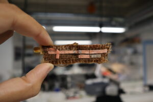
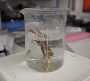
At the end of their lifespan, the boards can be degraded in hot water, while their copper tracks and integrated circuit chips delaminate and can be subsequently recycled.
Researchers from the University’s James Watt School of Engineering are working with Jiva Materials to unlock the full potential of the Soluboard in high-speed electronics operating at GHz frequencies. In a new white paper, the partners demonstrate how Soluboard can be used for radio frequency applications. They show that the PCBs can transmit signals at frequencies exceeding 4 GHz, which covers common wireless applications such as Wi-Fi, Bluetooth, and RFID. The paper also shows how Soluboard can support high-speed signals exceeding 3Gbits/s without any distortion, a range which could allow mainstream consumer electronics with interfaces such as HDMI and USB.
Accelerate your sustainability management and performance no matter where you are on your journey, learn more here!
“Working with natural and plant-based circuit materials is inherently challenging, particularly in wireless applications for RF and microwave applications,” says Dr. Mahmoud Wagih, Reader at the University of Glasgow’s James Watt School of Engineering. “The way forward is to co-design the materials with the specifications for meeting the wireless RF specifications. In this way, we can come up with antenna and radio designs which meet specific size and performance requirements.”
Reference: Wagih, Mahmoud et al. Biodegradable RF PCBs Towards Sustainable Wireless and IoT (doi: 10.36399/gla.pubs.368649).
https://eprints.gla.ac.uk/368649/2/368649.pdf
Ultra-low dielectric loss polymers for high-speed telecommunications
With the rollout of fifth-generation (5G) telecommunications networks and 6G, the demand for advanced materials that can handle high-frequency signals is rising rapidly. These systems use electromagnetic waves ranging from 10 to hundreds of gigahertz (GHz), where signals are highly sensitive to transmission loss, interference, and distortion. To address these issues, scientists and engineers rely on special insulating materials, known as dielectrics, which help guide signals with minimal loss.
Polymer-based dielectrics are particularly attractive. However, for high-frequency operation, they need two key traits: a low dielectric constant (Dk) and a low dissipation factor (Df). This is important for minimizing signal transmission loss in the GHz frequency range. Until now, polymer designs that simultaneously achieve both a low Dk and a low Df have been difficult to realise.
Now, a research team led by Professor Kenichi Oyaizu from the Department of Applied Chemistry, Research Institute for Science and Engineering at Waseda University in Japan, has developed a new class of polyphenylene sulfide (PPS) derivatives with ultralow dielectric loss. “Based on our previous research on high refractive index polymers, we hypothesized that replacing oxygen with sulfur in certain polymers, such as PPO, could significantly reduce the dissipation factor,” explains Oyaizu. “Using this strategy, we have succeeded in developing a new class of ultralow dielectric loss polymers.”
PPO (Poly(2,6-dimethyl-1,4-phenylene oxide)) is currently known to offer the best balance of a low Dk and Df. By replacing oxygen with sulfur in PPO, the researchers created PMPS (poly(2,6-dimethyl-1,4-phenylene sulfide)), a derivative of PPS. They studied the dielectric properties of PMPS at three different frequencies: 10 GHz, 40 GHz, and 80 GHz, and compared them with those of PPO. To further understand the role of sulfur, they also synthesized and studied two of its copolymers with PPO, referred to as P1 and P2, featuring an alternating sulfur and oxygen sequence.
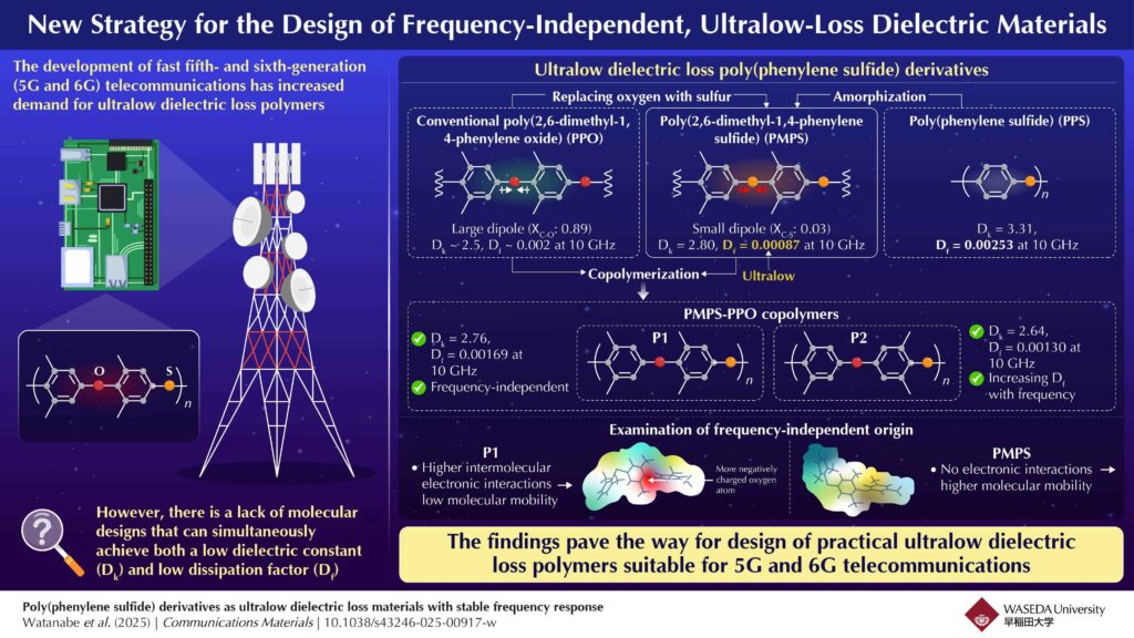
PMPS achieved a Dk of 2.80 and an ultralow Df of 0.00087 at 10 GHz, significantly lower than that of PPO. This improvement arises from the higher polarizability and smaller dipole moment (the measure of negative and positive charge separation) of the carbon–sulfur bond in PMPS compared to the carbon–oxygen bond in PPO. The copolymers also demonstrated excellent properties: P1 showed a Dk of 2.76 and Df of 0.00169, while P2 demonstrated a Dk of 2.64 and a Df of 0.00130. A comparison of the properties of PPO, PMPS, and its copolymers indicates that increasing sulfur content is a promising strategy for reducing Df.
The researchers also studied the frequency dependence of these properties over the 10–80 GHz range. While Dk values of all polymers did not change, Df showed an increasing trend for PPO, PMPS and P2. Interestingly, P1 retained an almost constant Df, achieving the lowest value among all polymers at 80GHz. This was due to the reduced motion between its molecules. Combined with strong thermal stability, this makes P1 a practical insulating material for future high-frequency telecommunications.
Reference: Seigo Watanabe et al. Poly(phenylene sulfide) derivatives as ultra-low dielectric loss materials with stable frequency response.
Communications Materials. DOI: 10.1038/s43246-025-00917-w
Caption: Replacing sulfur with oxygen in poly(2,6-dimethyl-1,4-phenylene oxide) leads to ultra-low dissipation factors. Moreover, the P1 copolymer exhibits a near-constant dissipation factor over a wide frequency range.
Light-harvesting devices and implantable electronics
Engineered polymers hold promise for use in next generation technologies such as light-harvesting devices and implantable electronics that interact with the nervous system. But creating polymers with the right combination of chemical, physical and electronic properties poses a significant challenge. New research offers insights into how polymers can be engineered to fine-tune their electronic properties to meet the demands of such specific applications.
“We are already building on this work to develop new materials for use in bioelectronic applications,” explains Aram Amassian, a professor of materials science and engineering at North Carolina State University. “That work is being done with collaborators from NC State, the University of Buffalo and the Karlsruhe Institute of Technology in Germany, with support from the National Science Foundation’s Designing Materials to Revolutionize and Engineer our Future program. Our goal there is to create organic bioelectronic materials that are ready for market adoption in healthcare and beyond.
“Silicon-based electronics have been around for decades, and we have a thorough understanding of the electronic properties of materials used in those technologies,” Amassian continues. “But we are now trying to develop a new generation of electronics that makes use of polymers in bioelectronics, though we do not yet have a detailed understanding of how the way we process and engineer polymers influences their electronic properties. That limits our ability to fine-tune the electronic properties of polymers to meet the demands of specific applications.”
To make electronically useful polymer materials, conjugated polymers that are able to carry a charge can be created. But to control the amount of charge that can be carried by the polymer, it must be doped – a process which involves incorporating a second molecule into the polymer in order to modify the material’s electronic properties.
“However, it’s not as simple as adding more doping agents if you want to increase the amount of charge the polymer can handle,” Amassian explains. “Electronic properties are affected by a range of variables and suffer when too much dopant is added. In fact, going into this study, we weren’t even entirely sure which variables were relevant, and which weren’t. Using conventional experimental techniques, it would basically take forever to figure it all out.”
 To that end, co-developers at Iowa State University created a system that made use of artificial intelligence (AI)-based algorithms and high-throughput processing to maximize experimental efficiency. This was used to understand how the processing, structure and electronic properties of doped polymers related to one another.
The so-called “DopeBot” system was tasked with producing the widest possible range of conductivities using a polymer called pBTTT and a doping agent called F4TCNQ. DopeBot then ran 32 experiments in which the pBTTT was doped with the F4TCNQ. Parameters that could be varied included the solvent used in the doping process and the temperature of the doping process.
The results of those reactions were characterized manually, and that characterization data fed back into DopeBot – which used those findings to inform what the next 32 experiments should be. This was done four times and repeated three more times with different parameters, meaning DopeBot conducted 224 experiments.
These experiments provided a tremendous amount of information: data on the parameters of all 224 experiments; data on the molecular and physical structure of the doped polymer that resulted from each experiment; and data on the electronic, optical and structural properties of the doped polymers.
Reference: Jacob Mauthe et al. AI-Guided High Throughput Investigation of Conjugated Polymer Doping Reveals Importance of Local Polymer Order and Dopant-Polymer Separation.
https://research.ncsu.edu/designing-polymers-for-use-in-next-generation-bioelectronics/
The views, opinions and technical analyses presented here are those of the author or advertiser, and are not necessarily those of ULProspector.com or UL Solutions. The appearance of this content in the UL Prospector Knowledge Center does not constitute an endorsement by UL Solutions or its affiliates.
All content is subject to copyright and may not be reproduced without prior authorization from UL Solutions or the content author.
The content has been made available for informational and educational purposes only. While the editors of this site may verify the accuracy of its content from time to time, we assume no responsibility for errors made by the author, editorial staff or any other contributor.
UL Solutions does not make any representations or warranties with respect to the accuracy, applicability, fitness or completeness of the content. UL Solutions does not warrant the performance, effectiveness or applicability of sites listed or linked to in any content.